The following program computes the square (k*k) of a positive integer k, stored in location 0x4000 and stores the result in location 0x4002. The result is to be treated as a 16-bit unsigned number.
Assumptions:
- A memory access takes 5 cycles
- The system call initiated by the HALT instruction takes 20 cycles to execute. This does not include the number of cycles it takes to execute the HALT instruction itself.
        .ORIG X3000
        AND R0, R0, #0
        LEA R3, NUM
        LDW R3, R3, #0
        LDW R1, R3, #0
        ADD R2, R1, #0
LOOP    ADD R0, R0, R1
        ADD R2, R2, #-1
        BRP LOOP
        STW R0, R3, #1
        HALT
NUM     .FILL x4000
        .END
- How many cycles does each instruction take to execute on the LC-3b microarchitecture described in Appendix C?
- How many cycles does the entire program take to execute? (answer in terms of k)
- What is the maximum value of k for which this program still works correctly?
- How will you modify this program to support negative values of k? Explain in less than 30 words.
- What is the new range of k?
- In which state(s) in the LC-3b state diagram should the LD.BEN signal be asserted? Is there a way for the LC-3b to work correctly without the LD.BEN signal? Explain.
- Suppose we want to get rid of the BEN register altogether. Can this be done? If so, explain how. If not, why not? Is it a good idea? Explain.
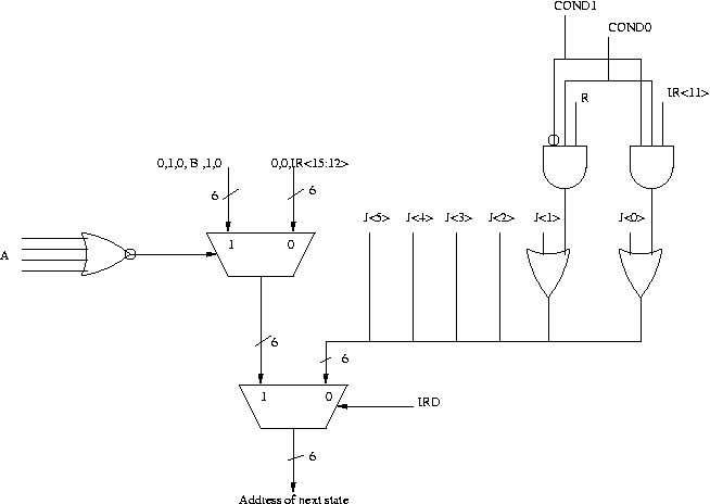
- Suppose we took this further and wanted to get rid of state 0. We can do this by modifying the microsequencer, as shown in the figure below. What is the 4-bit signal denoted as A in the figure? What is the 1-bit signal denoted as B?
Assembler Formats
ADDM DR, SR1, SR2
ADDM DR, SR1, imm5
Encodings

Operation
if (bit[5] == 0)
    DR = Memory[SR1] + SR2;
else
    DR = Memory[SR1] + SEXT(imm5);
setcc(DR);
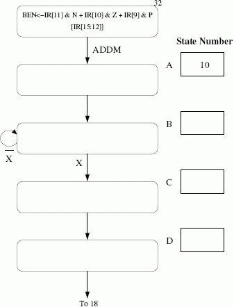
- We show below an addition to the state diagram necessary to implement ADDM. Using the notation
of the LC-3b State Diagram, describe inside each "bubble" what happens in each state, and assign
each state an appropriate state number (state A has been done for you). Also, what is the
one-bit signal denoted as X in the figure? Note: Be sure your solution works when the same
register is used for both sources and the destination (eg., ADDM R1, R1, R1).
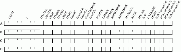
- Add to the Data Path any additional structures and any additional control signals needed to implement ADDM. Label the additional control signals "ECS 1" (for "extra control signal 1"), "ECS 2", etc.
- The processing in each state A,B,C,D is controlled by asserting or negating each control
signal. Enter a 1 or a 0 as appropriate for the microinstructions corresponding to states A,B,C,D.
- 16-bit address in MAR. This signal can take the following values: xFE00, xFE02, xFE04, xFE06, and OTHER (any other address between x0000 and xFDFF).
- 1-bit control signal R.W. The access is a read access if this signal is R, write access if it is W.
- 1-bit control signal MIO.EN. If this signal is 1, a memory or I/O access should be performed in this cycle.
The logic has five outputs:
- 1-bit MEM.EN signal. Memory is enabled if this signal is 1.
- 2-bit select signal for INMUX. This signal can take the following values: KBDR, KBSR, DSR, MEMORY.
- 1-bit LD.KBSR signal. KBSR will be load-enabled at the end of the current cycle if this signal is 1.
- 1-bit LD.DDR signal. DDR will be load-enabled at the end of the current cycle if this signal is 1.
- 1-bit LD.DSR signal. DSR will be load-enabled at the end of the current cycle if this signal is 1.
Your task is to draw the truth table for this Address Control Logic. Mark don't care values with X in your truth table. Use the conventions described above to denote the values of inputs and outputs. Please read Section C.6 in Appendix C on memory-mapped I/O before answering this question. Also, refer to Appendix A to find out the addresses of device registers.
     for(i = 0; i < 8; ++i){
       for(j = 0; j < 8; ++j){
         sum = sum + A[i][j];
       }
     }
The figure below shows an 8-way interleaved, byte-addressable memory.
The total size of the memory is 4KB. The elements of the 2-dimensional
array, A, are 4-bytes in length and are stored in the memory in column-major
order (i.e., columns of A are stored in consecutive memory locations) as shown.
The width of the bus is 32 bits, and each memory access takes 10 cycles.
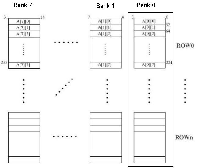
A more detailed picture of the memory chips in Row 0 of Bank 0 is shown below.
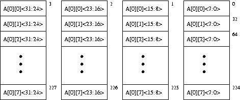
- Since the address space of the memory is 4KB, 12 bits are needed to uniquely
identify each memory location, i.e., Addr[11:0]. Specify which bits of the address
will be used for:
- Byte on bus
Addr[_____:_____]
- Interleave bits
Addr[_____:_____]
- Chip address
Addr[_____:_____]
- Row decode
Addr[_____:_____]
- Byte on bus
- How many cycles are spent accessing memory during the execution of the above code? Compare this with the number of memory access cycles it would take if the memory were not interleaved (i.e., a single 4-byte wide array).
- Can any change be made to the current interleaving scheme to optimize the number of cycles spent accessing memory? If yes, which bits of the address will be used to specify the byte on bus, interleaving, etc. (use the same format as in part a)? With the new interleaving scheme, how many cycles are spent accessing memory? Remember that the elements of A will still be stored in column-major order.
- Using the original interleaving scheme, what small changes can be made to the piece of code to optimize the number of cycles spent accessing memory? How many cycles are spent accessing memory using the modified code?
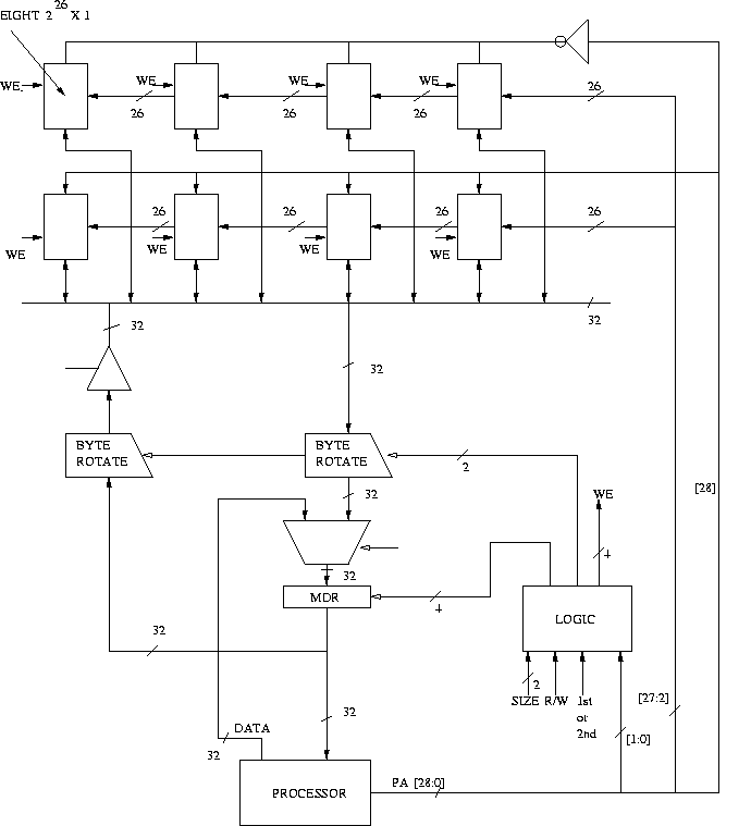
Construct the truth table to implement the LOGIC block, having inputs SIZE, R/W,
1st or 2nd access, PHYS_ADDR[1:0] and the outputs shown in the above figure. Assume
that the value of SIZE can be Byte (00), HalfWord (01), and Word (10). Clearly
explain what function each output serves.